They sit in the middle. Not quite a conductor like copper, not quite an insulator like rubber. This “intermediate space” makes semiconductor materials the backbone of every device we touch today.
Without these crystalline solids, we wouldn’t have smartphones in our pockets, servers running the Internet, and electric cars on the road. Diodes, transistors and integrated circuits are all based on them. They are small. They are reliable. And most importantly: you don’t waste a lot of energy.
Conductivity gap
Materials are usually divided into three categories.
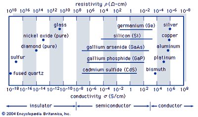
Insulators block electricity. Think fused silica or glass. Their conductivity is incredibly low, typically between $10^{-18} and $10^{-10} Siemens per centimeter. Conductors such as aluminum allow current to flow unimpeded. Their conductivity is high, typically $10^4$ to $10^6$ Siemens per centimeter.
Semiconductors live in a chaotic state between them.
The conductivity of a semiconductor is not fixed. It changes.
This variability is a feature, not a bug. Temperature. Light. Magnetic fields. Even the smallest impurities can radically change the semiconductor’s electrical conductivity.
Take silicon. It is the most common semiconductor material. Pure silicon is not particularly conductive. But if you add just a handful of boron atoms—about 10 boron atoms per million silicon atoms—the game changes completely.
This small addition, also called doping, increases electrical conductivity a thousandfold.
Why is this important? Because it allows engineers to create components with precise, controllable power handling characteristics. You can build transistors that act as switches or amplifiers. You can create optical sensors that detect light. You can make solid-state lasers that emit precise beams.
These separate components are useful. But their real strength is in integration. They can be tightly packed into microelectronic circuits. This integration enables modern computing. We are talking about complex systems that fit on a chip no bigger than a fingernail.
This scalability drives consumer and industrial markets. Semiconductors are key elements from signal processing to control systems. They are everywhere. And they will remain so for the foreseeable future.
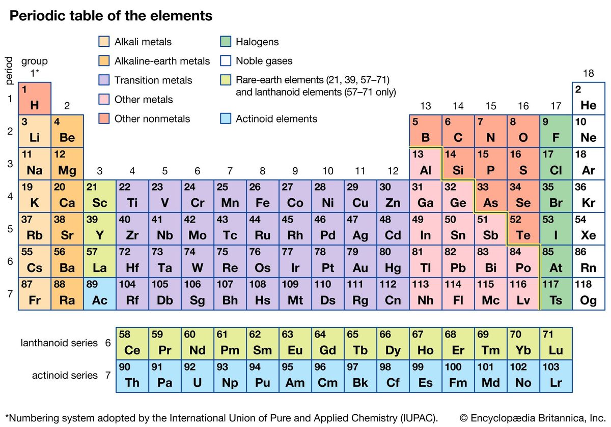
The story of semiconductors begins with atoms. In the early 1800s, researchers began to study the materials between conductors and insulators. The simplest ones are elemental. They consist of only one type of atom. Silicon (Si), germanium (Ge) and tin (Sn) belong to group IV of the periodic table of elements. Selenium (Se) and tellurium (Te) are in the sixth column.
But the real complexity comes from compounds. They are mixtures of two or more elements. Gallium arsenide (GaAs) is a binary III-V compound. It combines gallium from column III with arsenic from column V. You can get even more complex. Ternary compounds contain three elements. Mercury-indium telluride (HgIn2Te4) is an example of II-III-VI. In some cases, they may come from only two columns. Aluminum gallium arsenide (AlGaAs) is a ternary alloy of III-V groups. Aluminum and gallium are both in the third column. The ratio depends on the composition. If the subscript x is 1, it is pure aluminum. 0 means pure gallium.
Pure silicon is still the king of integrated circuits. However, in terms of luminescence, III-V binary and ternary compounds are dominant.
The Shift from Germanium to Silicon
Before 1947, semiconductors were simple. They were two-terminal devices. Use as a rectifier. Or as photodiodes. Then came the bipolar transistor. This changes everything.
In the early 1950s, germanium was the material of choice. It worked. But it had a flaw. Devices made of germanium have too much leakage current. Even at moderate temperatures, leakage is unacceptable in many applications.
Silicon came on the scene in the early 1960s. It quickly replaced germanium. The reasons were practical. First, silicon devices have much lower leakage currents. Secondly, silicon dioxide (SiO2) is easily formed on the silicon surface. Forms high-quality insulation. This makes manufacturing easier.
Today, silicon technology is everywhere. Silicon devices account for more than 95 percent of all semiconductor products worldwide.
Bright spots of compound semiconductors
Silicon is versatile. However, it is not suitable for all jobs. Many compound semiconductors have electrical and optical properties that silicon cannot match. Gallium arsenide is the most prominent example. It is better at handling light and certain radio frequencies.
This is why main computer processors do not find GaAs. You can find it in the field of optoelectronics. Found in RF applications. In these niche markets, the limitations of silicon become apparent.
材料选择如何定义设备性能
材料的选择不仅仅是学术性的。 它决定了设备实际可以做什么。 如果您需要处理数据,硅就是答案。 如果您需要发光或传输高频信号,您就会寻找其他地方。
这种分工解释了现代半导体的格局。 一种材料主导体积。 其他人主导特定领域的表现。 原子的物理性质决定了应用。
How atoms form a silicon base
Semiconductors are based on single crystals. Atoms arrange themselves in a tight three-dimensional network. In pure silicon, this structure is almost flawless.
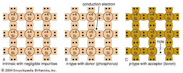
See a simplified 2D section of this crystal. Each silicon atom is surrounded by four neighbors. It has four outer electrons. It shares them. Each shared pair forms a covalent bond. The attraction between electrons and nuclei holds the lattice together.
Isolated atoms behave differently. They have separate energy levels. When you put many atoms together in a crystal, those levels spread out. They become energy bands.
Bandgap barrier
Temperature is important. At absolute zero, without thermal oscillation, electrons completely fill certain bands. The most filled band is the valence band. Above this is the conduction band.
There is a gap between them. A forbidden zone. Electrons cannot exist here. Insulators have a huge gap. Semiconductors have a smaller one. This bandgap determines the behavior of the material.
The most useful semiconductors are between 0.25 and 2.5 electron volts. Silicon is 1.12 eV. Gallium arsenide is 1.42 eV. Diamond, a perfect insulator, stretches to 5.5 eV. The size of this gap determines how easily current flows.
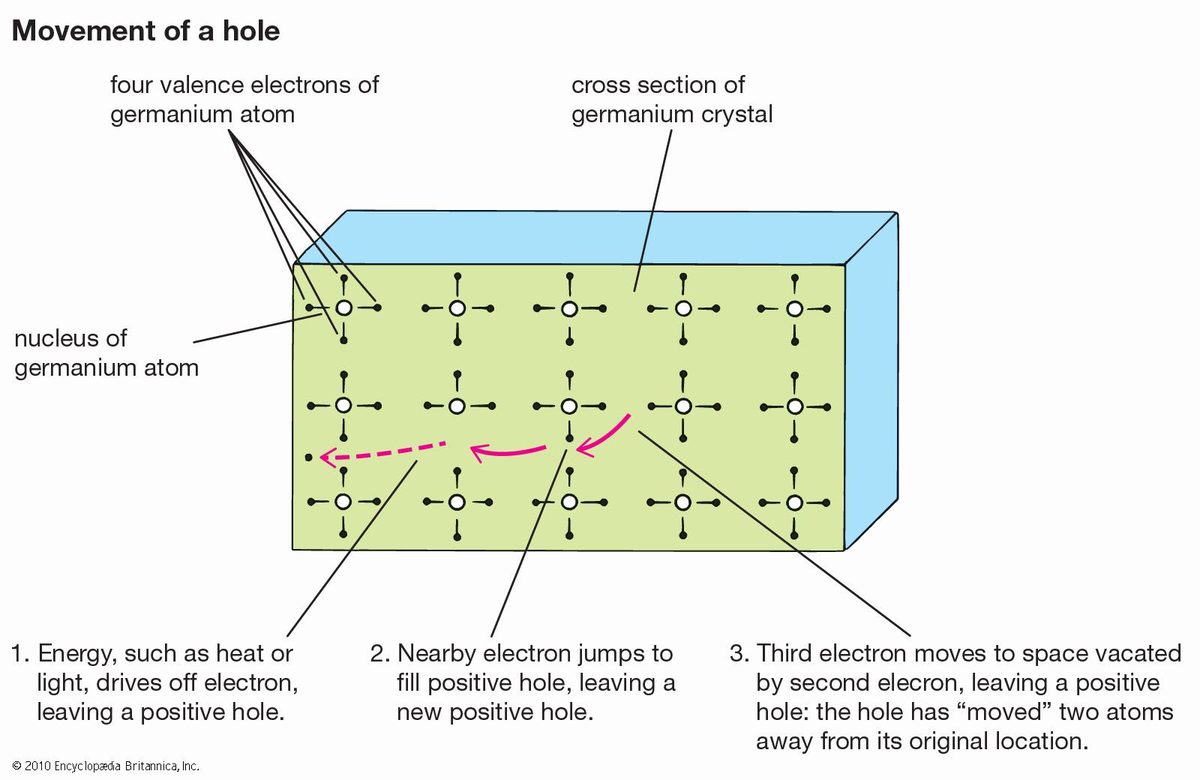
In a pure semiconductor, electrons become trapped at low temperatures. They sit in their assigned bands and are useless for conducting electricity. Heat changes that. Thermal vibrations can break covalent bonds and release electrons to carry electricity. But releasing an electron leaves a hole.
This vacancy is a “hole.”
Holes act like fictitious particles with a positive charge. They move in the opposite direction to electrons. When you apply an electric field, both free electrons in the conduction band and holes in the valence band move through the crystal. This dual movement creates current. Conductivity depends on two things: the density of these charge carriers and their mobility.
In a intrinsic semiconductor, the number of free electrons is equal to the number of holes. However, they do not move at the same speed. Electron mobility is typically higher. Take the intrinsic silicon at room temperature. Electrons zip along at 1,500 cm²/V·s. Holes lag behind at 500 cm²/V·s. Generally, when the temperature rises, the mobility drops for both.
Pure silicon conducts poorly at room temperature. To fix this, manufacturers dope it. They introduce impurities at about one part per million. This creates an extrinsic semiconductor. Doping boosts conductivity, although it slightly reduces mobility.
Creating n-type and p-type materials
Doping works by swapping atoms.
When you replace a silicon atom with a pentavalent atom, such as arsenic, four of its five outer electrons bond to neighboring silicon atoms. The fifth electron is free. It joins the conduction band. This creates an n-type semiconductor. Arsenic is a donor. It donates electrons.
If you replace silicon with a trivalent atom like boron, it only has three outer electrons. It requires a fourth to form stable covalent bonds. It steals an electron from a nearby bond. This creates a hole in the valence band. This creates a p-type semiconductor. Boron acts as a acceptor.
P-n junction
Where n-type and p-type materials meet, something interesting happens.
Diode effect and junction breakdown
When the impurity type inside the single crystal suddenly changes from p-type (acceptors) to n-type (donors), a p-n junction is formed. This is where the magic happens. On the P side, the holes are the dominant charge carriers, the so-called majority carriers. Some thermally generated electrons also stay there, acting as minority carriers. The N-side flips the script: electrons dominate, while holes are in the minority.
The depletion layer is located directly in the interface. Free charge carriers have been removed from this region, effectively converting the junction into an insulator. It’s a dead zone until an external voltage gets things going.
Rectification: How current flows in one direction
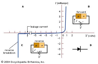
The defining property of a p-n junction is rectification. This allows current to flow easily in one direction while being blocked in the other direction. Look at the current-voltage curve of a silicon p-n junction : it’s not linear. It is stubborn.
If you apply a forward bias voltage – positive voltage on the p-side, negative on the n-side – the barrier collapses. Most of the majority carriers rush through the junction. A great current flows. Simply.
Reverse bias? Total opposites attract, but in this case they repel each other. The charge carriers move away from the junction and increase the depletion layer. Only a small leakage current sneaks through. It’s negligible. Until it isn’t.
Understanding Breakdown Voltage
Add reverse bias and the leakage current regrid constant. That is, until you reach a critical threshold. The junction collapses. The flow suddenly increases.
This junction breakdown is often harmless if you are manage the power dissipation. Don’t let it get too hot or the diode survives. It is not a failure; that’s the limit.
The forward voltage required to initiate a p-n junction is typically less than one volt. But reverse breakdown voltage? It varies greatly. In some devices, less than a volt. Thousands of volts to others. Impurity concentration and device parameters determine where this line is drawn.
Why this is important
One might think that p-n junctions are just abstract physics. They are not. They are the basis of modern electronics. Although there are more complex structures such as p-n-p and n-p-n transistors, they are all based on the basic behavior of a basic p-n junction.
Without this one-way valve, there is no rectification. There is no regulation. You don’t get integrated circuits that power everything from the phone to the grid. It is a simple structure. Sharp border. But it changes everything.
We’re still pushing the limits of how thin we can make these layers, how fast they can switch, and how much voltage they can withstand before breaking. The physics has not changed, but the applications are constantly expanding. Where will the next breakthrough come from?